
What Does 4x4x4 Mean on a TPU? Understanding TPU Slices and GPU Design Philosophy
When I first studied TPU architecture, slice specifications such as 4x4x4, 8x16, and 16x16 confused me. What exactly is being multiplied? Are these matrix dimensions? And why do TPU users need to think about topology when GPU clusters seem to hide it?
In Does AI Have Consciousness? Why ChatGPT Fails So Confidently 1, I described an LLM as a machine that uses matrix operations for probabilistic prediction. This article follows that computation one layer deeper into the hardware: when a matrix no longer fits on one chip, how does Google turn a mathematical problem into a data center wiring problem?
The short answer is that a TPU slice dimension such as 4x4x4 or 8x16 describes the physical topology of chips in the data center, not how a matrix is partitioned mathematically. Those are separate layers, and the XLA compiler maps one onto the other. Google chose 2D and 3D torus topologies instead of the expensive switched fabrics common in GPU clusters because of a fundamental tradeoff: more software and compiler complexity in exchange for better cost efficiency at hardware scale.
TL;DR: Four Core Takeaways
These are my notes after studying the subject:
- Deep learning is built around matrix multiplication: most forward- and backward-pass computation can be expressed as matrix operations, which is why TPU dedicates so much silicon to systolic arrays.
- A slice dimension is a wiring diagram, not a matrix partition: 4x4x4 describes 64 chips in a 3D grid. XLA decides how mathematical partitions are placed onto that physical topology.
- TPUs are not entirely switchless: copper directly connects chips within a cube, while OCS (optical circuit switching) connects cubes. TPU avoids expensive electronic packet switches; OCS and optical components account for less than 5% of total system cost.
- GPU topology complexity has not disappeared: GPU clusters put much of it into the hardware bill—NVSwitch and InfiniBand fat-tree fabrics. TPU reduces that hardware expense and shifts complexity to XLA and the engineers using it.
Why Deep Learning Depends on Matrix Multiplication
Each neural-network layer is fundamentally a linear transformation—inputs multiplied by weights and summed—followed by a nonlinear activation. Once an entire layer and a batch of examples are considered together, thousands of multiply-and-sum operations naturally become one matrix multiplication.
---
config:
  layout: dagre
  flowchart:
    curve: linear
    nodeSpacing: 15
    rankSpacing: 110
---
flowchart LR
    subgraph IN["Input layer (output of the previous layer)"]
        x1(("x1"))
        x2(("x2"))
        x3(("x3"))
    end
    subgraph HID["Hidden-layer neurons"]
        h1(("h1"))
        h2(("h2"))
        h3(("h3"))
        h4(("h4"))
    end
    subgraph OUT["Output layer (passed to the next layer)"]
        y1(("y1"))
        y2(("y2"))
    end
    x1 --> h1 & h2 & h3 & h4
    x2 --> h1 & h2 & h3 & h4
    x3 --> h1 & h2 & h3 & h4
    h1 --> y1 & y2
    h2 --> y1 & y2
    h3 --> y1 & y2
    h4 --> y1 & y2
Every arrow represents multiplication by a weight. A neuron’s output is the weighted sum of all incoming arrows followed by a nonlinear function. Taken together, a layer is an input vector multiplied by a weight matrix; stacking a batch of inputs produces a full matrix multiplication, X × W.
This packaging offers two major engineering benefits:
- Parallelism: the many multiply-accumulate operations are largely independent and can run on thousands of compute units at once, an ideal match for GPUs and TPUs.
- Data reuse: the same values are used repeatedly. Hardware can keep data moving and reuse it on-chip, reducing costly memory accesses. On modern chips, moving data often consumes far more energy than arithmetic itself.
Transformers and today’s LLMs ultimately do much the same thing: reduce attention and feed-forward networks to sequences of enormous matrix multiplications.
flowchart LR
    A["One neural-network layer<br>thousands of neurons × thousands of input dimensions"] --> B["Package as matrix multiplication<br>input matrix X × weight matrix W"]
    B --> C["Massively parallel hardware<br>GPU / TPU performs thousands of MACs at once"]
    C --> D["Reuse data while it moves on-chip<br>reduce memory traffic and energy"]
The Heart of a TPU: The Systolic-Array MXU
A TPU (Tensor Processing Unit) is Google’s accelerator for matrix operations—large numbers of multiplications and accumulations. Thousands of directly connected multiply-accumulate units form a large physical compute array.
Its core is the MXU (Matrix Multiply Unit), implemented as a systolic array 2. Think of it as a carefully scheduled factory line: weights are preloaded into a 2D grid of processing elements, while input values flow in wave after wave. Each element multiplies, accumulates, and passes data onward. Data “pulses” regularly through the grid without repeated memory reads and writes, making the design efficient and energy-conscious.
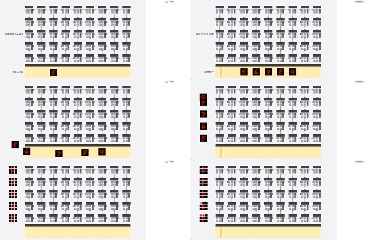
The TPU host streams data into an infeed queue. The TPU loads it into high-bandwidth memory (HBM), then loads parameters from HBM into the MXU for matrix operations. Results are written to the outfeed queue, where the host reads them into host memory.
The following table summarizes MXU specifications and network topology by generation 2 3 4 5 6 7 8 9:
| Generation | MXU specification | Network topology | Scale | Primary role |
|---|---|---|---|---|
| v1 (2015) | 256x256 (INT8) | Single chip | — | Inference |
| v2–v3 | 128x128 (BF16) | 2D torus | Up to 1,024 chips in a v3 Pod | Training |
| v4 (2021) | 128x128; four MXUs per TensorCore | 3D torus + OCS | 4,096-chip Pod | Flagship training |
| v5e | 128x128 | 2D torus | Up to 256 chips per slice | Cost-efficient training and inference |
| v5p | 128x128 | 3D torus + OCS | 8,960-chip Pod; largest slice 16x16x24 = 6,144 chips | Flagship performance |
| v6e (Trillium) | 256x256 | 2D torus | 256-chip Pod | 4.7× the peak compute of v5e |
| v7 (Ironwood / TPU7x, 2025) | 256x256 | 3D torus + OCS | 9,216-chip Superpod (also available as 256 chips) | Inference-era flagship; 42.5 ExaFLOPS FP8 peak per Superpod |
| v8 (TPU 8t / 8i, announced in 2026) | Not disclosed | New Boardfly topology for 8i; remaining details not fully disclosed | Not generally available yet | First split: 8t for training, 8i for low-latency inference |
Two details stand out:
- MXU dimensions remained 128x128 from v2 through v5p. Trillium (v6e) doubled them to 256x256, and Ironwood retained that size. Doubling each side quadruples the multiply-accumulate work per clock 2 7 10.
- This matters to programmers: matrix dimensions should ideally be multiples of 128—or 256 on v6e and TPU7x—to keep the MXU full. Otherwise, hardware pads with zeros and spends the same time computing unused values 10 11.
The newest generations show how topology is evolving. Ironwood (TPU7x, 2025) continues the 3D torus + OCS design, scaling one Superpod to 9,216 chips and 42.5 ExaFLOPS of peak FP8 compute. Larger systems connect multiple Superpods through the data center network (DCN) 8 12 13. The eighth generation, announced at Cloud Next 2026, splits into the training-focused TPU 8t and low-latency inference TPU 8i. For agentic AI workloads, 8i introduces the “Boardfly” topology, using direct optical paths to reduce the maximum chip-to-chip path from 16 hops to 7 9 14.
Training and inference have different communication patterns, so their optimal topologies are diverging. Topology is not dogma; it is cost engineering that evolves with the workload.
What Is a Slice? A Seating Chart for Chips, Not a Matrix Partition
Now we can return to the numbers in the title. For a v5e 8x16 slice, “8x16” means that 128 chips are arranged as an 8-row by 16-column physical grid. Each chip has high-speed ICI (Inter-Chip Interconnect) links to its neighbors above, below, left, and right 5. For a practical example, see GKE AI Series: Train Your First JAX Model on TPU 15.
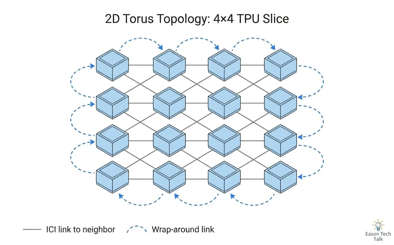
2D torus topology: a 4×4 slice, where each square is one TPU chip. Solid lines are direct ICI links to adjacent neighbors; dashed lines wrap the ends of every row and column together. An 8×16 slice works the same way with a larger grid.
The image uses a smaller 4x4 example. Each chip connects to four adjacent neighbors, and the ends of every row and column wrap around. That is a torus topology.
Chips with a 3D topology (v4 and v5p) have six ICI ports, connecting to one neighbor in each ±X, ±Y, and ±Z direction. Chips with a 2D topology (v5e and v6e) have four 4 11. Wrapping the edges prevents boundary chips from becoming isolated.
The primary motivation is lower latency, but the layout has several other benefits:
- Fixed chip degree keeps wiring predictable: every chip needs only four ports in 2D or six in 3D, enabling standardized, scalable hardware without connecting every chip to an expensive switch.
- More dimensions shorten communication distance: in a torus, the farthest path is roughly half the length of each dimension added together. Moving from a long 1D line to 2D or 3D sharply reduces worst-case hop count and gives collectives steadier bandwidth and latency.
- Collectives have natural paths: All-Reduce and All-Gather can use ring or mesh algorithms along the torus, passing data like a relay. This is well suited to regular deep-learning workloads.
The tradeoff is that software must understand the topology. A fat-tree or highly connected GPU network makes locality less visible to the programmer. On a TPU torus, however, parallel partitions need to align with physical neighbors. A poor mapping pushes traffic onto longer paths, which can delay synchronization, stall a job, or even deadlock an application.
From smallest to largest, the hierarchy looks like this:
flowchart TD
    A["TPU chip<br>contains TensorCore and MXU"] --> B["Tray<br>four chips paired with one CPU host"]
    B --> C["Rack<br>4x4x4 cube = 64 chips<br>copper-connected 3D grid"]
    C --> D["OCS optical circuit switching<br>connects cubes into a slice of the required size"]
    D --> E["Pod<br>v4: 4,096 / v5p: 8,960 / v7: 9,216 chips"]
    E --> F["Across Pods: data center network (DCN)<br>multislice training"]
For TPU v4, the base unit is a 4x4x4 cube of 64 chips in one rack, directly connected with inexpensive copper. OCS connects multiple cubes into larger slices. Slice dimensions can be various multiples of four—4x4x12 or 4x8x8, for example—and need not be powers of two 4 16. A v4 name such as v4-128 counts 128 TensorCores; with two TensorCores per chip, that is 64 chips, exactly one cube.
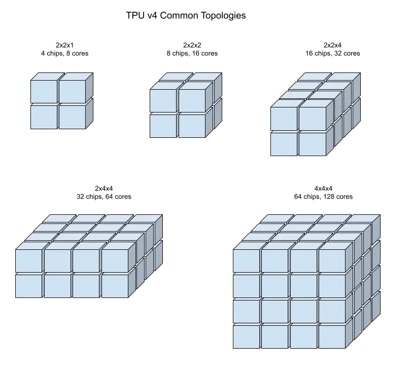
Common TPU v4 slice topologies, from 2×2×1 (4 chips) to one complete 4×4×4 cube (64 chips).
This brings us back to the original question: does the slice dimension describe how matrix multiplication is distributed? No. It is a physical seating chart for the chips.
Logical Mesh vs. Physical Topology: How XLA Maps Matrices to Chips
Once the physical seating chart is clear, the next question is how computation is placed onto it. Large-model training is typically partitioned along logical parallel dimensions. The two most common are:
- Data parallelism: different chips process different batches and synchronize gradients after each step.
- Model/tensor parallelism: a weight matrix is too large for one chip, so it is partitioned across several chips.
In JAX, this is commonly expressed as a logical mesh. For example, 128 chips might be declared as Mesh(('data', 'model'), (8, 16)): eight-way data parallelism by sixteen-way tensor parallelism 17.
The key is that the logical mesh and physical topology are different graphs; XLA maps the former onto the latter. Because ICI connects neighbors, distant chips communicate hop by hop 11. The compiler tries to map the logical axis with the most traffic to physically adjacent chips.
flowchart LR
    subgraph L["Logical layer (the mathematical problem)"]
        A["Enormous matrix multiplication"] --> B["Partition into parallel dimensions<br>data = 8, model = 16"]
    end
    subgraph P["Physical layer (data center wiring)"]
        C["8x16 chip grid<br>ICI connects adjacent neighbors only"]
    end
    B -->|XLA compiler mapping| C
    C --> D["Inside each chip<br>a 128x128 or 256x256 MXU performs the work"]
Consider an 8x16 v5e slice with a data = 8, model = 16 logical mesh. XLA can map data parallelism to one physical axis and tensor parallelism to the other. High-frequency tensor-parallel traffic then stays between adjacent chips, while the less frequent data-parallel gradient All-Reduce can travel efficiently around the torus.
In summary:
- Slice dimensions such as 8x16: physical wiring of the chip network.
- Matrix partitioning: mathematical tensor-sharding dimensions.
- What happens in practice: XLA maps the mathematical partition onto the physical topology to minimize path length. Regardless of the outer partition, each chip’s systolic-array MXU performs the actual arithmetic.
Why Not Use a Line? The Physical Limit of 1D Topology
Why make engineers reason about 2D and 3D layouts instead of arranging chips in one line? One dimension cannot support thousands of chips efficiently. In a line of 4,096 chips, the two ends are thousands of hops apart. Even after joining the ends into a ring, the farthest pair remains 2,048 hops apart. In a 16x16x16 3D torus, the maximum distance falls to 24 hops—at most eight in each dimension. More dimensions shorten average chip-to-chip distance.
GPU clusters are not 1D either; they simply hide more of the topology behind switching hardware. A typical NVIDIA DGX design uses NVSwitch to connect eight GPUs within a server, making them behave more like one large GPU. Across servers, leaf and spine InfiniBand switches form a fat-tree topology. The DGX SuperPOD reference architecture, for example, uses a three-level fat tree built with Quantum-2 InfiniBand 18. From the software’s perspective, the resulting network appears relatively flat.
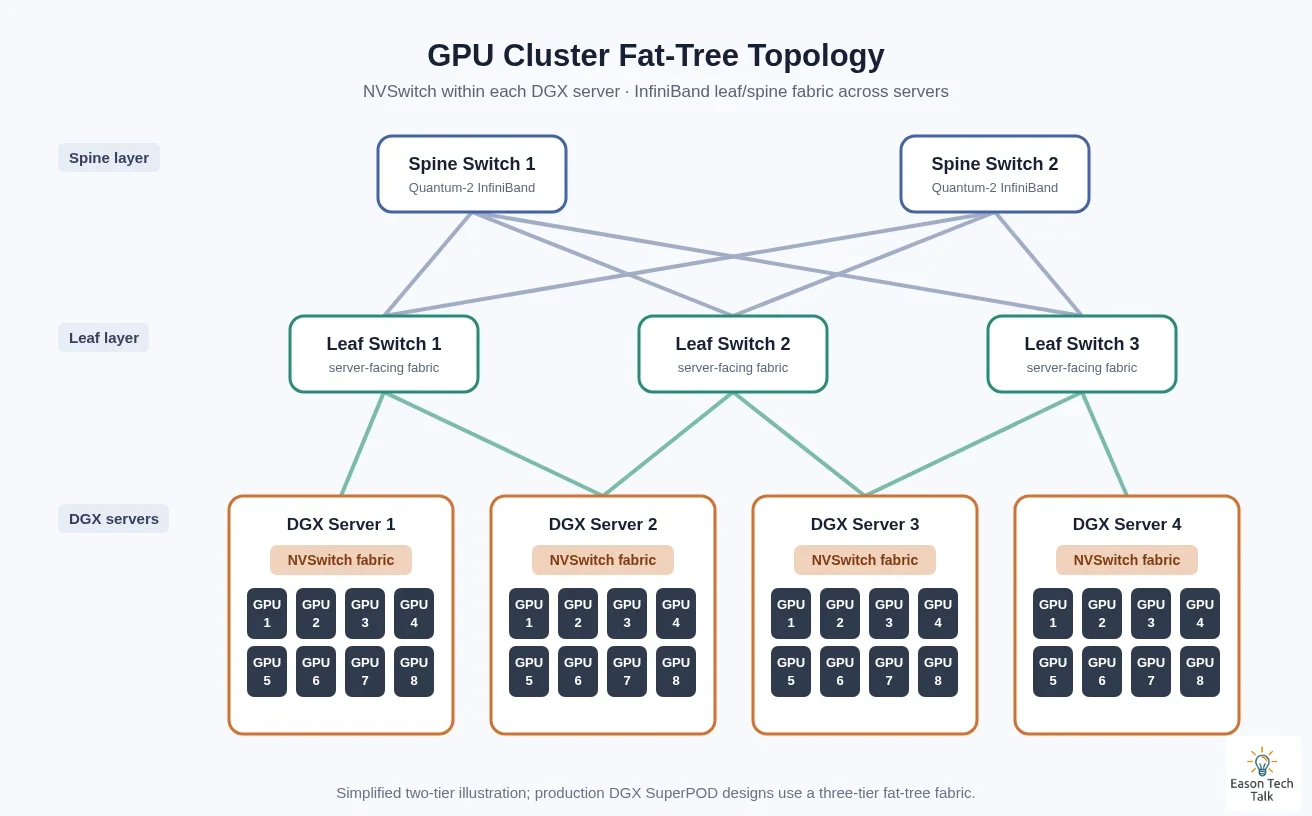
Simplified GPU cluster network: NVSwitch connects eight GPUs within each DGX server, while leaf and spine InfiniBand switches form a fat-tree topology across servers. Production SuperPOD designs use a three-tier fat tree.
That abstraction has a price. Maintaining nonblocking bandwidth between any pair of endpoints in a fat tree requires the number of switches, optical modules, and cables to grow rapidly. Network equipment is estimated to account for 15–20% of total GPU cluster cost, and the expense becomes more significant as the cluster grows 19.
TPU’s Cost-Saving Philosophy: ICI + OCS
This is where the TPU design makes a different tradeoff. It is not quite correct to say that TPUs use no switches 4:
- Within a 64-chip cube: passive copper cables connect chips through ICI as a 4x4x4 3D grid. This layer is genuinely switchless, or glueless.
- Between cubes: OCS (Optical Circuit Switching) connects them. A v4 Pod uses 48 OCS units to join 64 cubes, or 4,096 chips, into one system.
OCS is fundamentally different from an electronic packet switch such as InfiniBand. A packet switch resembles a mail-sorting center: it examines each packet’s address before deciding where to send it, requiring computation and adding latency and power use.
An OCS uses an array of adjustable MEMS mirrors to reflect light into another fiber. Once configured, the path behaves like a direct fiber: the OCS does not inspect or decode packets. This provides three important benefits 4:
- Low cost and power: OCS and the underlying optical components account for less than 5% of system cost and less than 3% of power.
- Reconfigurable topology: optical paths can form different slice shapes without recabling. They can even form a “twisted torus,” shortening paths for all-to-all traffic. A scheduler can deliver 4x4x12 when that is what a user needs.
- Fault tolerance and scheduling: paths can bypass a failed cube and use a spare. A scheduler does not have to find physically contiguous free chips; it can assemble available cubes into a slice.
The philosophies compare as follows:
| Feature | NVIDIA GPU cluster (NVLink / InfiniBand) | Google TPU slice (ICI + OCS) |
|---|---|---|
| Network topology | In-node NVSwitch connectivity plus an inter-node fat tree | Directional 2D / 3D torus mesh |
| Switching equipment | Many electronic packet switches | Direct copper within a cube; OCS optical paths between cubes |
| Network cost | Often estimated at 15–20% or more of cluster cost | OCS and optical components are less than 5% of system cost |
| Software complexity | Lower: topology is logically flatter and the CUDA ecosystem handles much of it | Higher: parallel axes must align with physical topology through XLA / shard_map |
| Flexibility | More uniform any-to-any bandwidth and broad applicability | Reconfigurable for workloads, failure bypass, and incremental deployment |
TPU exposes topology because of a deliberate tradeoff: it accepts software and compiler complexity in exchange for cost efficiency and flexibility at hardware scale.
This works because deep-learning communication is highly regular. On every step, chips repeatedly exchange data with predictable peers, such as during gradient synchronization. Torus networks excel at this neighbor-oriented traffic. The same design may be less attractive for general-purpose computation, where communication partners and timing are unpredictable and traffic may travel much farther across the mesh.
Conclusion
The reason a TPU slice is 4x4x4 is found not in a mathematics textbook but in data center wiring and infrastructure cost:
- The dimensions are a chip seating chart, not a matrix partition. 4x4x4 describes how 64 chips are arranged and wired. XLA maps the logical matrix partition to that physical chart.
- TPU saves on switching infrastructure. Copper connects chips inside a cube and OCS redirects optical paths between cubes. In v4, the entire optical system—OCS units, optical modules, and fiber—accounts for less than 5% of system cost. GPU clusters are estimated to spend 15–20% on networking such as InfiniBand fat trees, while NVSwitch is part of the server bill.
- Complexity moves; it does not disappear. Google’s hardware savings become work for the compiler and engineers: matrix dimensions should align to 128 or 256, and partitions should match physical topology. Otherwise the MXU may sit partly idle—or the job may stall entirely.
I hope this gives you a useful perspective on TPU architectural tradeoffs and helps you make more practical judgments when evaluating AI infrastructure or reading hardware specifications.
References
-
Further reading: Does AI Have Consciousness? Why ChatGPT Fails So Confidently ↩
-
TPU architecture (Google Cloud Documentation) - https://docs.cloud.google.com/tpu/docs/system-architecture-tpu-vm ↩ ↩2 ↩3
-
An in-depth look at Google’s first Tensor Processing Unit (Kaz Sato, Google Cloud Blog, 2017) - https://cloud.google.com/blog/products/ai-machine-learning/an-in-depth-look-at-googles-first-tensor-processing-unit-tpu ↩
-
TPU v4: An Optically Reconfigurable Supercomputer for Machine Learning (Jouppi et al., ISCA 2023) - https://arxiv.org/abs/2304.01433 ↩ ↩2 ↩3 ↩4 ↩5
-
TPU v5e (Google Cloud Documentation) - https://docs.cloud.google.com/tpu/docs/v5e ↩ ↩2
-
TPU v5p (Google Cloud Documentation) - https://docs.cloud.google.com/tpu/docs/v5p ↩
-
Introducing Trillium, sixth-generation TPUs (Google Cloud Blog, 2024) - https://cloud.google.com/blog/products/compute/introducing-trillium-6th-gen-tpus ↩ ↩2
-
TPU7x (Ironwood) (Google Cloud Documentation) - https://docs.cloud.google.com/tpu/docs/tpu7x ↩ ↩2
-
Our eighth generation TPUs: two chips for the agentic era (Google Blog, 2026) - https://blog.google/innovation-and-ai/infrastructure-and-cloud/google-cloud/eighth-generation-tpu-agentic-era/ ↩ ↩2
-
Cloud TPU performance guide (Google Cloud Documentation) - https://docs.cloud.google.com/tpu/docs/performance-guide ↩ ↩2
-
How to Think About TPUs — How To Scale Your Model (Google DeepMind) - https://jax-ml.github.io/scaling-book/tpus/ ↩ ↩2 ↩3
-
Ironwood: The first Google TPU for the age of inference (Google Blog, 2025) - https://blog.google/innovation-and-ai/infrastructure-and-cloud/google-cloud/ironwood-tpu-age-of-inference/ ↩
-
From silicon to softmax: Inside the Ironwood AI stack (Google Cloud Blog, 2025) - https://cloud.google.com/blog/products/compute/inside-the-ironwood-tpu-codesigned-ai-stack ↩
-
Inside the eighth-generation TPU: An architecture deep dive (Google Cloud Blog, 2026) - https://cloud.google.com/blog/products/compute/tpu-8t-and-tpu-8i-technical-deep-dive ↩
-
Further reading: GKE AI Series: Train Your First JAX Model on TPU ↩
-
TPU v4 (Google Cloud Documentation) - https://docs.cloud.google.com/tpu/docs/v4 ↩
-
Manual parallelism with shard_map (JAX documentation) - https://docs.jax.dev/en/latest/notebooks/shard_map.html ↩
-
GPU Cluster Network Topology Design: Fat-Tree, Dragonfly, and Rail-Optimized Architectures (Introl, 2025) - https://introl.com/blog/gpu-cluster-network-topology-fat-tree-dragonfly-rail-optimized-2025 ↩
-
Network Bandwidth — The Hidden Bottleneck in AI Infrastructure (Medium) - https://medium.com/@indiai/network-bandwidth-the-hidden-bottleneck-in-ai-infrastructure-e60e4d17093a ↩